This accurate model of a varactor diode should help designers of voltage-controlled oscillators (VCOs).
![]()
Millimeter-wave frequency bands are attractive for their wide available bandwidths. There are a number of ways to generate these signals but, for each type of oscillator, it is desirable to be able to tune the source electronically, as well as in a defined and controlled manner. By using a suitable reactive device (such as a varactor diode) for tuning these millimeter-wave oscillators, the relationship between an applied voltage and the resulting frequency can be precisely defined. This can aid the design engineer in achieving the required spectral performance at these higher frequencies.
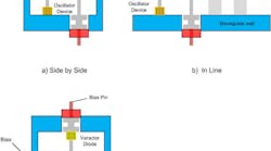
Oscillators developed for use at millimeter-wave frequencies are typically designed around waveguide housings. Electronic tuning of a waveguide-type oscillator can be accomplished in a number of ways, some of which are shown in Fig. 1. Additional information can be found in the technical literature (ref. 1) and in a recent article (ref. 2). The tuning sensitivity of a millimeter-wave varactor-tuned oscillator (VTO) can be estimated by means of relatively simple models, and this article hopes to provide some sights into the tuning relationship. Usually, the approach is to keep the fixed capacity with the varactor diode as large as possible, using the varactor diode to control the resonant frequency to the greatest extent.
1. These three VCO configurations show the circuits (a) side by side, (b) in line, and (c) stacked.
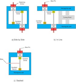
A varactor diode is essentially an active device with positive-negative (PN) junction which has reverse bias applied. This results in a movement of charge carried away from the junction, so that this region is referred to as the depletion layer. The depletion layer has charge on either side of the junction and acts like a parallel-plate capacitor (Fig. 1). The capacitance relationship for a parallel-plate capacitor is C = εA/W, where:
A = the effective cross-sectional area of the device,
ε = the relative dielectric constant of the depletion layer, and
W = the width of the depletion layer.
Application of a voltage results in an increase of the depletion layer width, affectively altering the capacitance (Fig. 2).
2. These drawings show the depletion layer of a varactor diode (left) and how its capacitance can change with applied voltage (right).
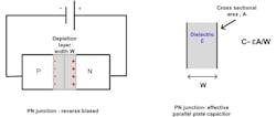
The typical fabrication process for a varactor diode results in a device with a mesa structure. This device can be mounted in a number of different standard and custom housings to simplify handling. The junction capacitance and associated parasitic circuit elements can be included in a simple equivalent circuit (Fig. 3) for modeling and simulation purposes.
3. The drawing (left) represents a packaged diode along with its equivalent circuit (right).
The selection of a suitable semiconductor device for a varactor diode can make an impact on the performance of the diode, although this receives little coverage in the literature. Varactors are true diodes with a clearly defined junction, which can be characterized by means of a particular doping profile; this is effectively captured in the gamma parameter for each varactor diode. The gamma parameter can be placed in two categories: abrupt and hyperabrupt. Quite simply, a varactor diode is effectively a variable reactance which is a function of some applied DC tuning voltage. More detailed models of varactor diodes are available in the literature, which are useful for a specific package or unpackaged devices. To obtain a general understanding of a varactor diode’s behavior, it is a reasonable to ignore packaging and parasitic affects in the first instance, as this allows the designer to appreciate the merits of such devices.
This basic approach leads to the following expression:
V = control voltage;
Cv = varactor capacitance; and
Γ = the gamma or doping profile.